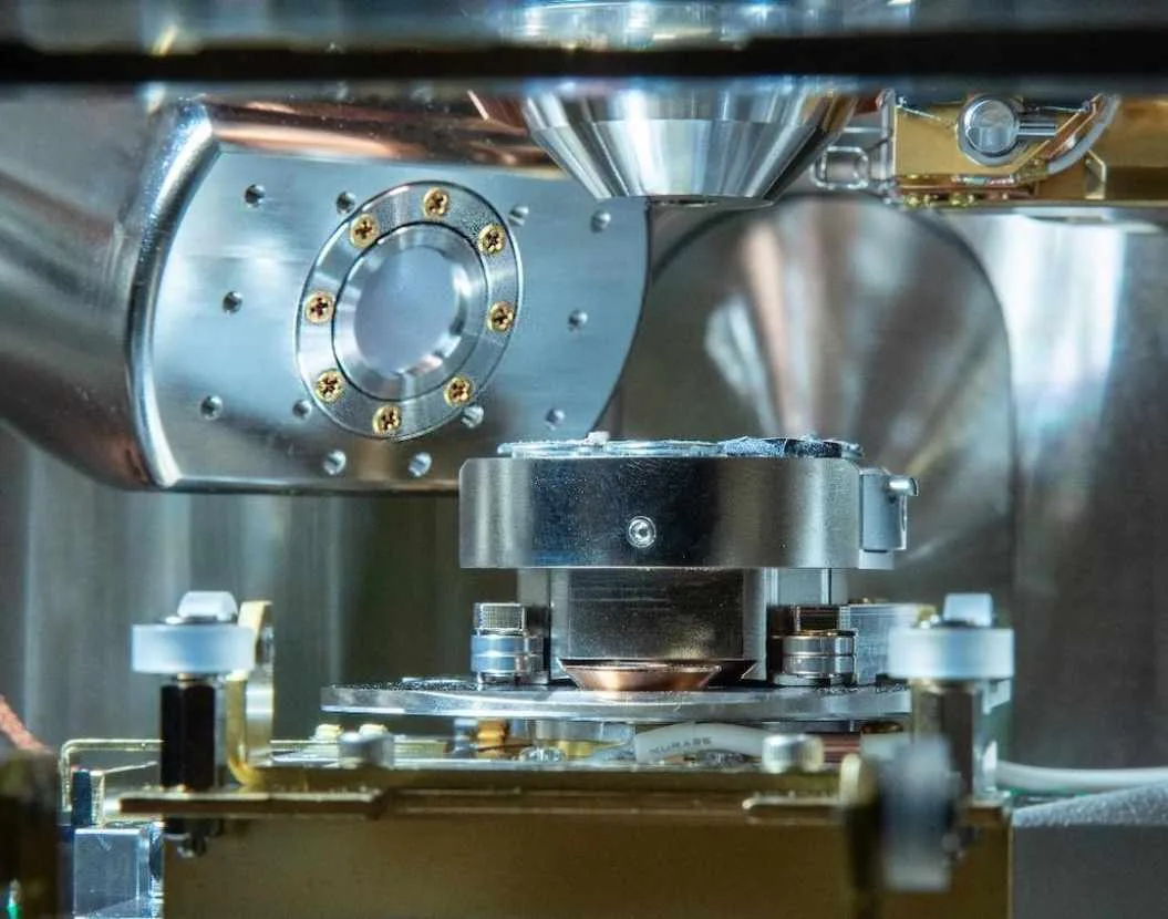

A new Hyperspectral X-ray Imaging (HXI) detector that enables highly sensitive analysis of the elemental and chemical composition of diverse materials has been developed by a group of researchers at Los Alamos National Laboratory.
With an energy resolution 20 times superior to the presently accessible commercial technology, the detector created by the team enables manufacturers to detect crucial defects on silicon microchips during quality assurance before mass production, while also offering the capability to detect material defects at the nanoscale before constructing bridges or airplanes.
Matt Carpenter of Los Alamos’ Safeguards Science and Technology group says HXI represents a generational leap forward in energy resolution and efficiency for material analysis in scanning electron microscopes.
“This allows researchers to measure detailed composition at the nanoscale in ways never before possible.” he said
In various fields like geology, environmental science, forensics, semiconductor fabrication industry, and materials engineering, microanalysis of material composition through X-ray spectroscopy in scanning electron microscopes (SEMs) is a routine practice. However, existing commercial detectors used for measuring X-ray spectra necessitate users to prioritise either high-energy resolution or high detection efficiency.
Consequently, a detailed mapping of chemical and elemental composition of material at the nanoscale level was not feasible until recently.
This type of microanalysis is particularly crucial for samples that exhibit compositional variations on minuscule length scales and where the macroscopic characteristics are reliant on microscopic features.
Los Alamos National Laboratory, National Institute of Standards and Technology, and the University of Colorado developed the Hyperspectral X-ray Imaging detector, or HXI, to meet this analytical challenge.
Electron microscopes are crucial tools
In all the aforementioned areas of research, electron microscopes play a vital role. Incorporating the HXI detector with a standard scanning electron microscope uncovers intricate details about materials and objects at the nanoscale, which are thousands of times smaller than what can be seen by a light-based optical microscope.
When the electron beam of the microscope interacts with the sample, X-rays are produced, each possessing energies distinctive to an individual element.
The X-ray spectrum can be used to determine the elemental composition of the sample, which, when combined with the electron beam’s spatial information, can create a map down to the nanometer level.
This technique is broadly applicable across various scientific and industrial domains, such as measuring nanometer-sized chip features for semiconductor manufacturing, analyzing alloy nanoscale structure for materials science, and studying small-scale mineral structure and distribution for geology and mineral exploration.
Operating the HXI detector
Operating the HXI detector resembles how commercial energy dispersive X-ray spectrometers (EDS) operate, exhibiting high efficiency across the entire X-ray energy range.
Furthermore, the energy resolution of HXI equals or surpasses that of a wavelength dispersive spectrometer (WDS). HXI seamlessly integrates the advantages of both into an innovative instrument, an accomplishment that had not been achieved before.
Increased visibility into a material leads to a better understanding of its properties, allowing for potential enhancements. The HXI detector also provides essential insights to promote the development of next-generation technologies worldwide.