
In a game-changing breakthrough, scientists at the Department of Energy’s Oak Ridge National Laboratory (ORNL) have cracked open a new frontier in semiconductor technology.
Their groundbreaking study unveils how subtle tweaks in the isotopic composition of ultrathin semiconductor materials can wield astonishing influence over their optical and electronic properties, potentially paving the way for a quantum leap in semiconductor design.
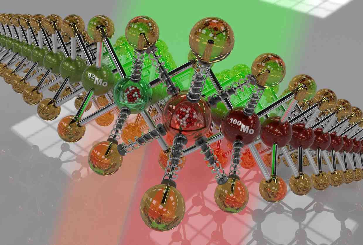
Semiconductors are the unsung heroes powering our digital age, driving the evolution of electronics and computing. Now, ORNL researchers have pushed the boundaries of possibility by harnessing the power of isotopes – variants of elements with different masses – to engineer semiconductors with unprecedented precision.
Lead scientist Kai Xiao said, “We observed a surprising isotope effect in the optoelectronic properties of a single layer of molybdenum disulfide, an effect that opens opportunities to engineer 2D optoelectronic devices for microelectronics, solar cells, photodetectors, and even next-generation computing technologies.”
The study’s lead author, Yiling Yu, spearheaded the cultivation of isotopically pure 2D molybdenum disulfide crystals, unveiling a remarkable discovery: even minor alterations in the isotopic makeup of these materials can lead to profound shifts in their behavior.
Notably, crystals with heavier isotopes emitted light skewed towards the red end of the spectrum, defying conventional wisdom and pointing to a new frontier in semiconductor physics.
Xiao and his team, in collaboration with theorists at the University of Central Florida, delved deep into the underlying mechanisms, uncovering how crystal vibrations influence the behavior of optical excitations within these ultrathin crystals.
“Unexpectedly, the light from the molybdenum disulfide with the heavier molybdenum atoms was shifted farther to the red end of the spectrum, which is opposite to the shift one would expect for bulk materials,” Xiao said
The newfound understanding holds the key to unlocking a wealth of new applications, from advanced photovoltaics to cutting-edge quantum technologies.
The implications are profound, suggesting that isotope engineering could revolutionise semiconductor design, offering unparalleled control over their optical and electronic properties.
Looking ahead, Xiao and his team are poised to embark on further collaborations, leveraging ORNL’s state-of-the-art facilities to explore the isotope effect’s impact on spin properties for potential applications in spin electronics and quantum emission.
The groundbreaking research, published in Science Advances, received support from DOE’s Office of Science, Basic Energy Sciences, Materials Sciences and Engineering Division, and was conducted at ORNL’s Center for Nanophase Materials Sciences (CNMS), an Office of Science user facility.
The CNMS played a pivotal role in facilitating various measurements critical to the study, underscoring the collaborative effort driving this semiconductor revolution.